
Synthesis, Structural and Optical Characterization of CdS and ZnS Quantum Dots
Rana Hamood
Affiliation
1Physics Department, Faculty of Science, Assiut University, Egypt
2Nanomaterials Lab., Physics Department, Faculty of Science, South Valley University, Qena-83523, Egypt
Corresponding Author
Rana Hamood, Physics Department, Faculty of Science, Assiut University, Egypt. Email: rananom77@yahoo.com
Citation
Rana Hamood. Synthesis, Structural and Optical Characterization of CdS and ZnS Quantum Dots. (2018) J Nanotechnol Material Sci 5(1): 16-22.
Copy rights
© 2018 Rana Hamood. This is an Open access article distributed under the terms of Creative Commons Attribution 4.0 International License.
Keywords
CdS; ZnS; Quantum dots; XRD; HRTEM; Optical properties.
Abstract
In the present work CdS and ZnS nanoparticles (NPs) were synthesized by organometallic method. The structural
properties of CdS and ZnS nanoparticles were determined by X-ray Diffraction (XRD), High resolution transmission
electron microscope (HRTEM) and their optical properties by UV-Visible and PL (Photoluminescence) analyses. XRD
analysis showed the prepared samples as hexagonal structure with particles size in the range of 2.62 – 2.73 nm for CdS
and of 1.92-2.73 for ZnS NPs. The HRTEM analysis revealed the formation of ZnS nanoparticles with uniform shape
and size. FTIR properties were measured for identification of chemical bonds in the nanomaterial, while Raman spec-
troscopy is studied the confinement of the optical phonon modes in the QDs. The UV-Visible absorption showed the
blue shift in the band gap of CdS and ZnS NPs from those of the corresponding bulk materials which could be traced
back to the quantum confinement effect. The PL emission measured for (excitation at 350 nm) for ZnS showed compar-
atively3-foldenhancements from CdS NPs (excitation at 450 nm).
Introduction
Due to their electronic and fascinating optical properties, semiconductor quantum dots based on luminescence properties of II - VI group’s elements have gained considerable attention to research community[1-5]. Because of their fundamental role in basic research and technological applications, synthesis and characterization of discrete nanostructures is of significant importance[6]. Regarding their particle applications, it is a generally recognized fact that large surface to volume ratio that the nano structure spossess enhanced surface effects resulting novel phenomena. Accordingly, Nano building materials such as ZnO nanowires, GaN nanowires, ZnS nanoparticles, CdS nanoparticles and Carbon nanotubes are intensively investigated[5,6]. At the nanoparticles sizes of semiconductors, some of the physical properties noticeably differ from those of the corresponding bulk materials, for instance, the energy gap increases and the optical spectrum is shifted toward the short-wavelength region[7].
Cadmium sulfide (CdS) nanoparticles possess various applications in display devices, solar cells and as photocatalyst[8,9]. Resent research on nanoparticles has shown that they could stand as potential candidates for electronic and optoelectronic applications. It is worth mentioning too, that synthesis, characterization and studies of optical properties of cadmium sulfide have been researched, analyzed and described by several research groups[10-13]. CdS is a wide band gap semiconducting material having bandgap energy of 2.42 eV and it’s widely used because of its size dependent photo physical and non-linear optical properties etc.[14-16]
Zinc sulfide (ZnS) is an important II-VI group semiconductor material with a direct band gap of 3.7 eV and is widely used as phosphor in photoluminescence (PL), electroluminescence (EL) and optical sensor because of its chemical stability compared to those other chalcogenides such as ZnSe[1]. It further, exhibits wide optical transparency from the visible light (0.4 μm) to the deep infrared region (12 μm) which makes ZnS as one of the most promising materials among II-VI groups.
The synthesis of CdS and ZnS nanoparticles has been prepared by many various methods, some of which are the direct reaction of metals with sulfur powder under high temperature; the thermal decomposition of molecular precursors containing M-S bonds[17]; the use of poisonous H2S as S2- source at higher temperature[18] and finally the chemical co- precipitation method[19].
In this work, CdS and ZnS nanoparticles have been synthesized by organometallic method[20] using CdO and ZnO as precursors and TOPO (Trioctylphosphine oxide) as capping agent to control the particle sizes. The crystallinity and morphology have been studied by using X-ray powder diffraction (XRD) and high-resolution transmission electron microscope (HRTEM). The vibrational structure and the changes of the optical properties with particle size have been approved by using FTIR and Raman spectroscopy. The UV- visible spectra and the photoluminescence (PL) emission properties of CdS and ZnS samples are presented.
Experiment
Synthesis of CdS and ZnS Nanocrystals by Organometallic Method
Pure Sulfur powder as a Sulfur source, and all the chemicals that will be mentioned later are of analytical grade and used without further purification. The experimental setup that has been used in the preparation of CdS and ZnS nanoparticles consisted of a glass round bottom flaskon heating mantle maintained at 170°C. CdO and ZnO were used as starting materials to synthesis CdS and ZnS NPs by various sizes. The weight amounts of 0.3 g CdO or ZnO have been solved in (3 ml) Oleic acid, then heated up to 170°C with continuous stirring. A mixture of (2g) TOPO and (2g) HDA (Hexadecylamine) has been added and then the temperature has been increased up to 220°C. When the solution became transparent, the temperature was decreased to 190°C.Trioctylphosphine sulfur (TOP-S) solution was injected. Four samples of CdS and ZnS nanocrystals were withdrawn at different time intervals (5, 15, 20 & 30 min) and labeled from (ato d) for CdS and from (1 to 4) for ZnS. Drawn samples were cooled and diluted by addition of toluene. The samples b of CdS and 2 of ZnS were centrifuged at (4000 rpm, 15 min) and the obtained precipitates were washed three times by acetone and methanol. The obtained powders are characterized by XRD to confirm the crystalline phase and size.
Results and Discussion
Structural and Morphology
The typical XRD pattern of the prepared samples of CdS and ZnS nanoparticles is shown in (Figure 1). XRD were determined by using wide-angle X-ray scattering; Philips PW 1710 monochromatic Cu-Kα radiation with (λ = 1.54056 Å). The diffraction peaks were indexed to hexagonal phased of CdS and ZnS QD’s with major (hkl) peaks at (002), (110) and (112) respectively, and the lattice constants were found to be a = 4.15, c = 6.78 for CdS while a = 3.83, c = 6.38 for ZnS as represented in JCPDS cards nos.(04-017-1120) (04-017-6151) respectively. The XRD peaks were found to be broad indicating the nanocrystalline behavior of the particles. The average crystalline sizes of the samples were determined from the full width at half maximum of the (002) peak making use of Scherrer’s equation[21].
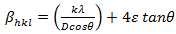
L = Kλ/βD cosθ…… (1)

Figure 1: X-ray powder pattern diffraction collected on two different samples: CdS (sample b) and ZnS (sample 2) nanoparticles.
In which L is the coherence length, βhkl is the full width at half maxima (FWHM) of the diffraction peak (in radian), λ is the X-ray wavelength, θ is the angle obtained from 2θ value corresponding to maximum intensity peak pattern and K is the geometric factor (0.9). In case of a small crystallites; L = 3/4 D, where D is diameter of nanoparticles. The estimated particle size for CdS was 3.34 nm while its value for ZnS was 2.95 nm. The measured lattice constants, d-spacing and particles size were reported in (Table 1).
The strain and grain sizes of both samples CdS and ZnS were calculated by Williamson-Hall (W-H) method. In general, the local distortion of the lattice has generated strain in the lattice. Its contribution to peak broadening is well known as strain broadening. By considering the strain to be uniform deformation model (UDM) in all crystallographic directions, the strain broadening can be written as:
 ………….. (2)
The significant property of Equation (2) is the dependency on the diffraction angle θ. The Williamson-Hall method does not follow a 1/cosθ dependency as in the Scherrer equation, it instead varies with tanθ. This fundamental difference allows for a separation of reflection broadening when both micro structural causes-small crystallite size and micro strain-occur together. The distinct θ dependencies of both effects laid the basis for the separation of size and strain broadening in the analysis of Williamson and Hall[22] results in the following equations:
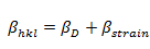
βhkl = βD+ βstrain …………. (3)
By substituting the values for βD and βstrain in Equation (3)
 ……… (4)
By rearranging Equation(4) we get:
 ……. (5)
A W-H plot is drawn with 4 sin ϴ along the x-axis and βhkl cosθ along the y-axis for the prepared CdS and ZnS NPs as it is shown in (Figure 2a,b). From the linear fit to the data, the particle size D has been estimated by the Y-intercept and the strain was calculated from the slope of the graph. It has been observed that the particle size that has been calculated from the Scherrer’s equation is in close agreement with the particle size estimated from the W-H plot. The calculated average crystallite sizes obtained from Scherrer method and UDM model with strain are listed in (Table 1).
Table 1: The X-ray analysis of CdS and ZnS nanoparticles by Scherrerand Williamson-Hall.
| Sample | 2θ °of the intense peak |
FWHM (degree) | (hkl) | d-spacing (Å) Std. |
d-spacing (Å) Obs. |
a (Å) | c (Å) | Scherrer equ. | Williamson-Hall method | |
|---|---|---|---|---|---|---|---|---|---|---|
| D (nm) | D (nm) | (no unit) | ||||||||
| CdS | 26.2 | 3.58 | (002) | 3.32 | 3.37 | 4.15 | 6.78 | 3.34 | 2.02 | 1.78 |
| ZnS | 28.24 | 4.23 | (002) | 3.15 | 3.16 | 3.83 | 6.38 | 2.95 | 3.73 | 1.27 |
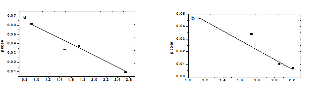
Figure 2: The W-H analysis of (a) CdS, (b) ZnS.
(Figure 3a,b) indicates the energy representative spectrum (EDS) of the CdS and ZnS nanoparticles which have been investigated by EDS (JEOL JSX 3222 element analyzer). It shows the unambiguous evidence for the presence of Cd/ S and Zn/S components. It has been found that atomic weight ratios of Cd and S in the CdS NPs were around 58.93% and 41.07%, respectively, while the atomic weight ratios of Zn and S in the ZnS NPs were around 72.79% and 27.21%, respectively. From the EDS spectrum, no impurities have been observed in the structure.
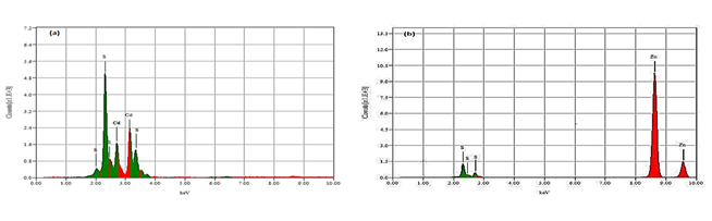
Figure 3: EDX spectrum of (a) CdS and (b) ZnS NPs.
(Figure 4a, b) shows the high-resolution transmission electron microscopy (HRTEM) images for CdS and ZnS NPs with their particles size distribution determined by using (JEM-2100 of 200 KV). In (Figure 4a), it has been observed, too, in CdS that the shape of the nanoparticles is nearly spherical with some agglomeration. It has been inferred from the histogram that the mean particle diameter is about 3.5 ± 0.5 nm. The obtained value of the d-spacing calculated for CdS is equal to 0.20 nm corresponding to (110) plane. (Figure 4b) shows homogenous distribution of ZnS NPs with no agglomeration. The lattice planes distance is identical to hexagonal ZnS, its calculated value equals to 0.24 nm corresponding to (102) plane, and its average size from the histogram is equal to 3.3 ± 0.3 nm.
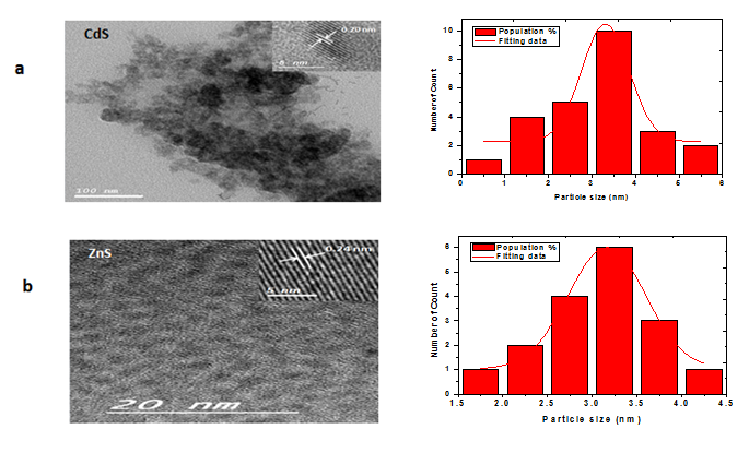
Figure 4a, 4b: HRTEM images and size histogram for synthesis (a) CdS and (b) ZnS nanoparticles.
It has been noticed that the particle size measured from TEM micrograph is larger than that value calculated from XRD. This might be explained by the fact that the X-ray detects only the crystalline part of the particles. X-ray size corresponds to the size of the crystalline regions within the particles and not to the effective particle size. So, the results for Scherrer’s equation can be seen as a lower limit of the particle size. (Figure 5a, b) shows the FTIR spectrum of TOPO capped CdS and ZnS nanoparticles at room temperature which was recorded by using (FT/IR spectrometer -4100 LE) in the range of 4000 - 500 cm-1. The observed vibration peaks at (2929 & 2849 cm-1) and at (2919 & 2847 cm-1) are attributed to C-H stretching bands that confirm the capping of alkyl group over CdS and ZnS NPs, respectively. The peaks at 2354 cm-1 for CdS and 2499 cm-1 for ZnS are due to C-N vibrations. The peaks are observed at 1568 cm-1 for CdS and at 1557 cm-1 for ZnS NPs which are corresponding to C-O stretching, respectively. Peaks appeared at 1493 cm-1 for CdS and at 1466 cm-1 for ZnS are attributed to COOH stretching. The peaks at 1062 cm-1 for CdS and 1047 cm-1 for ZnS are due to the presence of resonance interaction between vibrational modes of sulfide ions in the crystal. The peaks appearing at 723 cm-1 for CdS and at 731 cm-1 for ZnS are assigned to Cd-S and Zn-S stretching vibrations.
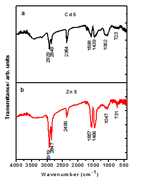
Figure 5: FTIR spectra for the prepared CdS and ZnS NPs.
(Figure 6 a, b) shows the Raman spectrum of CdS and ZnS nanoparticles at room temperature. In (Figure 6a), one peak is located at 235 cm-1 which corresponds to transverse optical (TO) phonon mode and two peaks are located at 368 & 560 cm-1 which correspond to fundamental bands related to stretching vibrations of longitudinal optical (LO) phonon modes of CdS 1LO and 2LO, respectively.
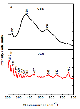
Figure 6: Raman spectra for the prepared CdS and ZnS NPs.
(Figure 6b) shows a peak that at 210 cm-1 is attributed to the second order of longitudinal acoustic (2LA) phonon mode. The band at 240 cm-1 can be attributed to the combination of two phonons at w (2(0) at w). The peak appearing at 274 cm-1 represents transverse optical (TO) phonon mode. The two other bands occur at 300 and 315 cm-1 are assigned to the same surface optical (SO) mode. The weak peak at 343 cm-1 is assigned to longitudinal optical mode (LO). The combination bands at 363, 437 and 567 cm-1 can be assigned to TO+LA, LO+TA and 2TO-TA, respectively. The peaks at 640 and 750 cm-1 correspond to 2TO and 2LO modes, respectively. Raman spectra were recorded using Brucker Senerra Raman microscope (Bruker Optics Inc., Germany) with 785 nm excitation.
Optical Properties
The effect of time and concentration on the optical properties of the prepared samples were evaluated by using a Perkin Elmer lambda 750 UV-V is spectrophotometer in the wavelength range 200 - 900 nm. The optical absorbance versus wavelength traces for prepared CdS and ZnS nanoparticles samples have been recorded, as it is shown in (Figure7 a, b). The position of the peaks and wavelengths located at (449 nm to 454 nm) for CdS and at (293 nm - 312 nm) for ZnS as particle size is increased. The absorption spectrum of CdS and ZnS nanoparticles shifted towards the lower wavelength side is attributed to the quantum size effect. Concerning the peak position, in (Figure 7a) one could roughly estimate the average size of CdS QDs from the following Yu’s et al. equation[23].
D = (-6.6521 × 10⁻⁸) λ3+ (1.9557 × 10⁻⁴) λ2 - (9.2352 × 10⁻²) λ + 13.29 (6)
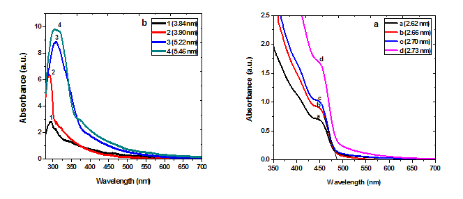
Figure 7: UV-Visible spectra of different samples of (a) CdS and (b) ZnS nanoparticles.
In which D (nm) is the size of a given nanocrystal sample and λ (nm) is the wavelength of the first excitonic absorption peak of the corresponding sample. Whereas the average particle size of ZnS QDs could be estimated from the following equation[24,25].
 (7)
(7)
In which r is the particle size that has been calculated as a function of peak absorbance wavelength (λp) for ZnS NPs. The calculated diameters of CdS are (2.62 - 2.73 nm) and of ZnS are (1.92 to 2.73 nm). The deviation of the peaks in absorption spectra is about 5 nm for CdS and 19 nm for ZnS, which might be due to the difference of the surface states of these QDs as it is shown in (Table 2). The estimated size by HRTEM is in good agreement with the size calculated by XRD. These results are similar to those previously reported[26].
Table 2: Spectroscopy parameters of CdS& ZnS Nanoparticles.
| CdS | ZnS | ||||||||||||
|---|---|---|---|---|---|---|---|---|---|---|---|---|---|
| Samp. No. | Reaction time (min) | Abs.λ WL nm | Emission λmax nm | Particle size nm by Yu Eq. | X-ray size nm | HRTEM size nm | Samp. No. | Reaction time (min) | Abs.λ WL nm | Emission λmax nm | Particle size nm byλmaxEq. | X-ray size nm | HRTEM size nm |
| a | 5 | 449 | 456 | 2.62 | - | - | 1 | 5 | 293 | 454 | 1.92 | - | - |
| b | 15 | 451 | 460 | 2.66 | 3.34 | 3.5 | 2 | 15 | 294 | - | 1.95 | 2.95 | 3.25 |
| c | 20 | 453 | 464 | 2.70 | - | - | 3 | 20 | 310 | 463 | 2.61 | - | - |
| d | 30 | 454 | 470 | 2.73 | - | - | 4 | 30 | 312 | 466 | 2.73 | - | - |
The absorption which corresponds to electron excitation from the valance band to conduction band can be used to determine the nature and values of the optical band gap. The relation between the absorption coefficient (α) and the incident photon energy (hν) can be written as[27].
(αhν) = K(hν-Eg )n …….. (8)
Where K, h, and Eg are a constant, the Planck’s constant and the band gap respectively. For n = 1/2, Eg in Eq. 1 is the direct allowed band gap. To measure the energy band gap of CdS and ZnS NPs from the absorbance spectrum a graph (αhν)2 versus hν is plotted in (Figure 8). The extrapolate of the straight line to (αhν)2 = 0 axis represents the value of CdS and ZnS which have been found to be 2.73 eV and 3.97 eV respectively. These values are blue shifted from that of bulk values (498 nm, Eg = 2.49 eV) for CdS and (340 nm, Eg = 3.65 eV) for ZnS, (Table 3).
Table 3: Band gap increment in CdS, ZnS quantum dots due to quantum confinement.
| Sample | Absorption edge nm | Band gap in eV | Increment in band gap eV |
|---|---|---|---|
| CdS Bulk | 498 | 2.49 | - |
| ZnS Bulk | 340 | 3.65 | - |
| CdS Nano | 454 | 2.73 | 0.24 |
| ZnS Nano | 312 | 3.97 | 0.32 |

Figure 8: Variation of (αhν)2 with hν for CdS and ZnS NPs as a function of wavelength at n value of 1/2.
The absorption edge shifts towards the lower value of wavelength (higher energy) for ZnS rather than CdS samples. The increasing band gap for ZnS NPs is due to the more occurring quantum confinement.
The room-temperature photo-luminescent (PL) spectra of the prepared CdS and ZnS Quantum Dots (QDs) measured by using JASCO-FP-6300 fluorescence spectrometer were shown in Figure. 9a, b. Excellent capping of (TOPO) is effectively passivated CdS and ZnS samples. In the present investigation, fluorescence spectra were performed with an excitation wavelength of λex = 450 nm for CdS and 350 nm for ZnS.
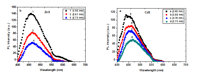
Figure 9: Photoluminescence intensity of (a) CdS (b) ZnS nanoparticles at various sizes.
The emission band maximum for CdS is observed between 456 nm and 470 nm at sizes ranging from 2.62 nm to 2.73 nm while for ZnS it is observed between 454 - 466 nm for sizes ranging from 1.92 - 2.73 nm. The peak positions of CdS and ZnS spectra are blue shifted compared to their corresponding bulks. Both samples show red shift gradually as the particle size increase.
(Figure 10) the photoluminescence (PL) spectra of the CdS and ZnS NPs have been determining by strong emission peaks at around 459 nm and 457 respectively. This strong emission is attributed to deep trap sites which in turn could be traced back to sulfur vacancies. The PL of ZnS NPs is blue shifted (2 nm) compared with the PL of CdS NPs. Interesting result of the work can be seen from PL emission spectra, that is the emission intensity of capped ZnS sample is significantly high in comparison to capped CdS nanoparticles about 3-fold increment in intensity has been achieved, that is because ZnS is optically transparent to the emission range, therefore no photons losses associated to ZnS with visible light emission[28].
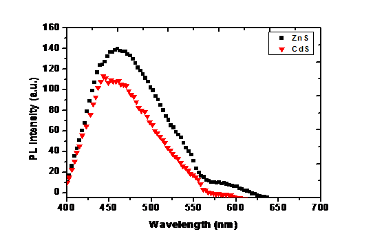
Figure 10: The PL spectra of CdS and ZnS nanocrystals.
Conclusion
Various sizes (1.92 - 2.73 nm) for CdS and ZnS NPs were prepared successfully by organometallic method. The wurtzite structure of CdS and ZnS NPs could be observed in most particle size range. The size of nanocrystalline powder was about 3.34 nm for CdS and about 2.95 nm for ZnS. Williamson-Hall analysis were used to study the individual continuation of crystallite size and lattice strain on peak broadening on CdS and ZnS NPs. TEM images of CdS and ZnS nanocrystals revealed the spherical shape and the crystallinity. FTIR and Raman spectra of the samples supported the formation of CdS and ZnS nanoparticles. The optical properties of the nanoparticles were extensively characterized by UV-Vis absorption and photoluminescence spectroscopy. Absorption peaks were blue-shifted gradually as the particle size decreased indicating quantum size effect by forming smaller particles. The optical gap of CdS NPs was around (2.73 eV) which was differ from that of ZnS NPs (3.97 eV). It has been noticed that, the optical band gap values of prepared samples are effectively tuned by the particle size. Therefore, there was enhancement of the band gap by 0.24 eV for CdS and 0.32 eV for ZnS NPs corresponding to the bulk. ZnS NPs resulted better enhancement of the photoluminescence than that of CdS NPs.
References
- 1. Bodo, B., Kalita, P.K. Chemical Synthesis of ZnS:Cu Nanosheets. (2010) AIP Conf. proc 1276: 31-36.
- 2. Denzier, D., Olschewski, M., Sattler, K. Luminescence studies of localized gap states in colloidal ZnS nanocrystal. (1998) J. Appl. Phys 84 (5): 2841-2845.
- 3. Zhang, H., Chen, X., Li, Z., et al. Preparation of sensitized ZnS and its photocatalytic activity under visible light irradiation. (2007) J. Phys. D: Appl. Phys 40(21): 6846-6849.
- 4. Lu, H.Y., Chu, S.Y. The mechanism and characteristics of ZnS-based phosphor powders. (2004) J. Cyst. growth. 265(3-4): 476-481.
- 5. Peng, H., Liuyang, B., Lingjie, Y., et al. Shape Controlled Synthesis of ZnS Nanostructures: A simple and Rapid Method for one Dimensional Materials by Plasma. (2003) Nanoscale Res. Lett 4(9): 1047-1053.
- 6. Srinivas, V., Barik, S.K., Bodo, B., et al. Magnetic and electrical properties of oxygen stabilized nickel nanofibers prepared by the boro hydride reduction method. (2008)J. Magn. Magn. Mater. 320(6): 788-795.
- 7. Borah, J.P., Sarma, K.C. Optical and Optoelectronic Properties of ZnS Nanostructured Thin Film. (2008) Acta. Phys. Polon. A. 114: 713-719.
- 8. Lahewil, A.S., Al-Douri Y., Hashim, U., et al. Structural and optical investigations of cadmium sulfide nanostructures for optoelectronic applications. (2012) Solar Energy. 86: 3234–3240.
Pubmed||Crossref||Others
- 9. Chate, P.A., Patil, P.A.S., Patil, J.S., et al. Synthesis, optoelectronic properties and photoelectrochemical performance of CdS thin films. (2013) Physica B: Condens. Matter 411(15): 118-121.
- 10. Khan, Z.R., Zulfequar, M., Khan, S.M. Optical and structural properties of thermally evaporated cadmium sulphide thin films on silicon (1 0 0) wafers. (2010) Mater. Sci. Eng B 174(1-3): 145-149.
- 11. Khomane, A.S. Morphological and opto-electronic characterization of chemically deposited cadmium sulphide thin films. (2010) J. Alloys. Compd. 496 (1): 508-511.
- 12. Seoudi, R., Shabaka, A.A., Kamal, M., et al. Dependence of spectroscopic and electrical properties on the size of cadmium sulfide nanoparticles. (2012) Physics E. 45: 47-55.
- 13. Elango, M., Nataraj, D., Prem Nazeer, K., et al. Synthesis and characterization of nickel doped cadmium sulfide (CdS: Ni2+) nanoparticles. (2012)Mater. Res. Bull 47 (6): 1533-1538.
- 14. Alivisatos, P. Semiconductor Clusters, Nanocrystals, and Quantum Dots. (1996) Science 271: 933 -937.
- 15. Soloviev, V.N., Eichhofer, A., Fenske, D. Size-Dependent Optical Spectroscopy of a Homologous Series of CdSe Cluster Molecules. (2001) J. Am. Chem. So. 123(10): 2354-2364.
- 16. Kim, J. I., Jung, D., Kim, J., et al. Surface–plasmon-coupled photoluminescence from CdS nanoparticles with Au films. (2012) Solid State Commun. 152(18): 1767-1770.
Pubmed||Crossref||Others
- 147. Wang, C.Y., Mo, X., Zhou, Y., et al. A convenient ultraviolet irradiation technique for in situ synthesis of CdS nanocrystallites at room temperature. (2000)J. Mater. Chem 10: 607-608.
Pubmed||Crossref||Others
- 18. Pickeet, N. L., Foster, D.F., Cole Hamilton, D.J. Effect of pyridine upon gas-phase reactions between H2S and Me2Cd; control of nanoparticle growth. (1996) J. Mater. Chem. 6(3): 507-509.
- 19. Singh, V., Chauhan, P. Structural and optical characterization of CdS nanoparticles prepared by chemical precipitation method. (2009) J. Phys. Chem. Solids. 70(7): 1074-1079.
- 20. Murray, C.B., Norris, D.J., Bawendi, M.G. Synthesis and characterization of nearly monodisperse CdE (E = sulfur, selenium, tellurium) semiconductor nanocrystallites. (1993)J. Am. Chem. Soc. 115(19):8706-8715.
- 21. Cullity, B.D. Elements of X-Ray Diffraction, second ed. (2003) Addison-Wesley Company, USA. 102.
Pubmed||Crossref||Others
- 22. Prabhu, Y. T.,Rao, K.V., Kumar,V.S., et al. X-Ray Analysis by Williamson-Hall and Size-Strain Plot Methods of ZnO Nanoparticles with Fuel Variation. (2014) World J NanoSci Eng. 4(1): 21-28.
- 23. Yu, W.W., Qu, L., Guo, W., et al. Experimental Determination of the Extinction Coefficient of CdTe, CdSe, and CdS Nanocrystals. (2003) Chem. Mater 15(14): 2854-2860.
- 24. Tiwari, A., Khan, S.A., Kher, R.S. Surface characterization and optical properties of polyphosphate capped ZnS nanoparticles. (2011) Adv. Appl. Sci. Res., 2(1): 105-110.
Pubmed||Crossref||Others
- 25. Abbas, N.K., Al- Rasoul, K.T., Shanan, Z. J. New Method of Preparation ZnS Nano size at low pH. (2013) Int. J. Electrochem. Sci 8: 3049–3056
Pubmed||Crossref||Others
- 26. Iranmanesh, P., Saeednia, S., Nourzpoor, M. Characterization of ZnS nanoparticles synthesized by co-precipitation method. (2015) Chin. Phys. B. 24 (4): 046104(1-4).
- 27. Muthukrishnan, S., Subramaniam, V., Mahalingam, T., et al. EFFECT OF AL Doping on Structural, Optical, Electrical and Photo-Catalytic Properties of CUO Nanoparticles. (2017) IJARR 2(2): 51-64.
Pubmed||Crossref||Others
- 28. Kumar, H., Barman, P.B., Singh, R.R. Development of CdS, ZnS Quantum Dots and their Core/Shell structures by wet chemical method. (2014) Int. J. Sci. Eng. Res. 5(5): 40-53.
Pubmed||Crossref||Others